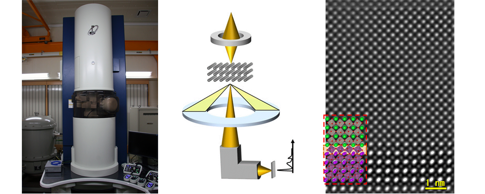
High Spacial and Energy Resolution Analysis using Scaning Transmission Electron Microscopy (STEM) and Electron Energy-Loss Spectroscopy
In the field of nanotechnology,the importance of high spacital resolution
analysis of material further increase.In general, X-ray diffraction method is used to know the atomic structure
of the crystal. However, since the diffraction method reflects average
strucrure derived fromperiodical structure of crystal, it is difficult to know non-periodic local structure such as crystal
defect and interface. On the other hand, since electron microscopy can
intuitively know local structure in real space, it is widly used and essential
analytical tool in recent nanotechnology field. In addition, the combination
with enery dispersive X-ray spectroscopy (EDS) and electron energy-loss
spectroscopy (EELS) can know the information of elemental and electronic
state with atomic scale. In our laboratory, we are studing material science
with atomic scale and necessary analytical method using (scanning) transmission
electron microscopy ((S)TEM) combined with EDS and EELS technique.